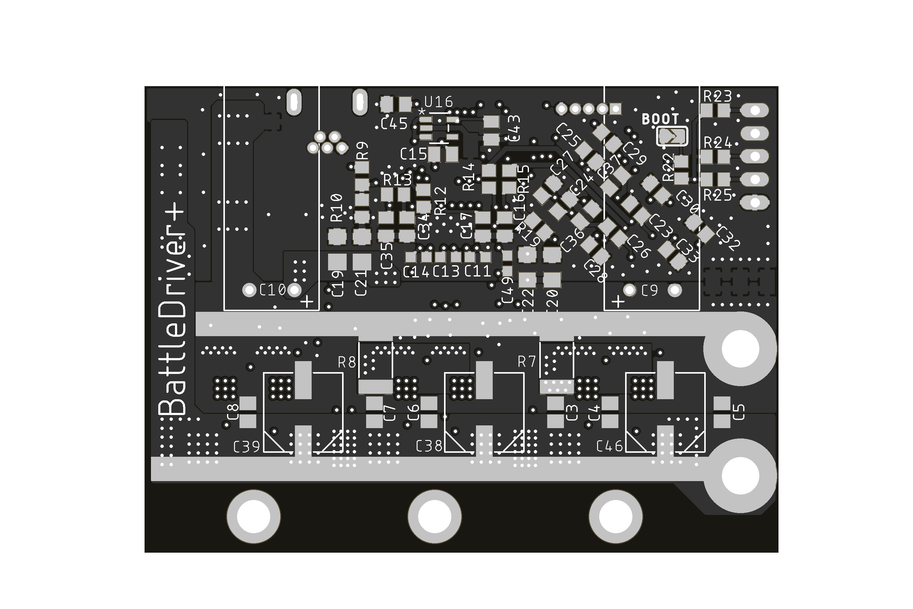
This design is based off the original BattleDriver HW V1.0, and has 12 mosfets for powering the motor, as compared to the previous 6 mosfets. The increase in mosfets have made the board a bit larger, at 70mm x 51mm, instead of 45mm x 70mm. In addition to the larger footprint, the board will be slightly thicker, as the BattleDriver+ has dual radial electrolytic capacitors (1mF at 35v) on the bottom to provide additional bypass capacitance for the mosfets. This board will be 23mm thick at the thickest portion, as compared to 14mm on the original BattleDriver. These additional radial capacitors can be removed to reduce the thickness of the board, down to the same as the original BattleDriver if the extra capacitance is not needed.
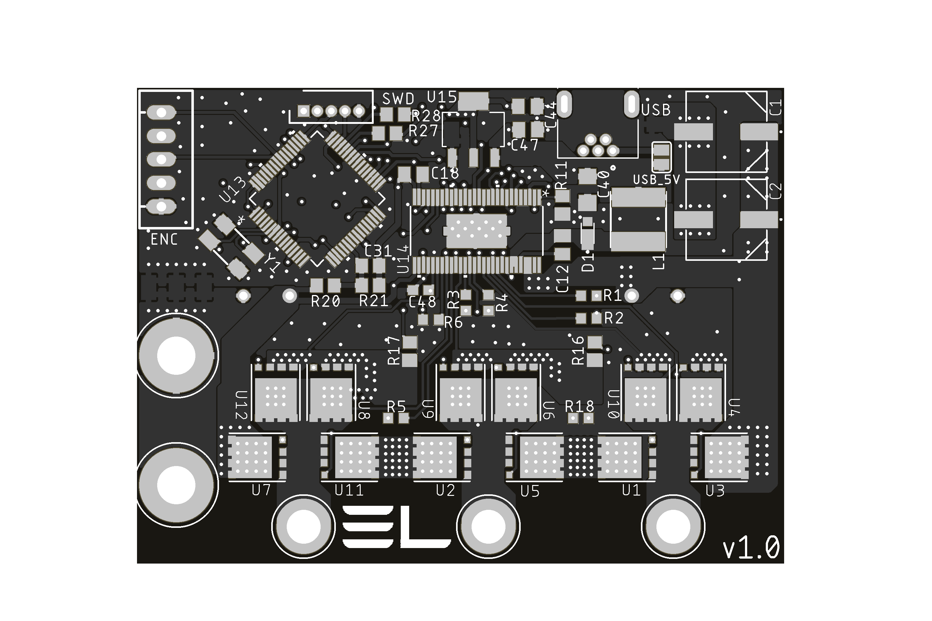
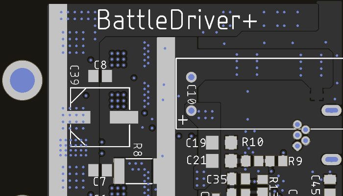
The layout of the board is designed with thermals and current capacity in mind. The mosfet layout is such that heat sinks can be easily placed to cover either each phase separately, or to cover high/low side mosfets individually. Further, each mosfet has at least 9 thermal vias to carry heat to the bottom of the board to improve unassisted heat dissipation.
The power section of the board should be able to handle very high currents, as all mosfets have a significant amount of vias, as well as very wide traces (7.5mm) to carry the current. Beyond this, both the PGND and PVDD traces have exposed copper to allow a bare solid core (~12AWG) wire to be soldered directly to the power rails to further aid in carrying current to each phase.
Similarly to the original BattleDriver, this board has a dedicated stackup and separated ground nets in an attempt to reduce switching noise throughout the board (and especially in the analog current sense circuits).
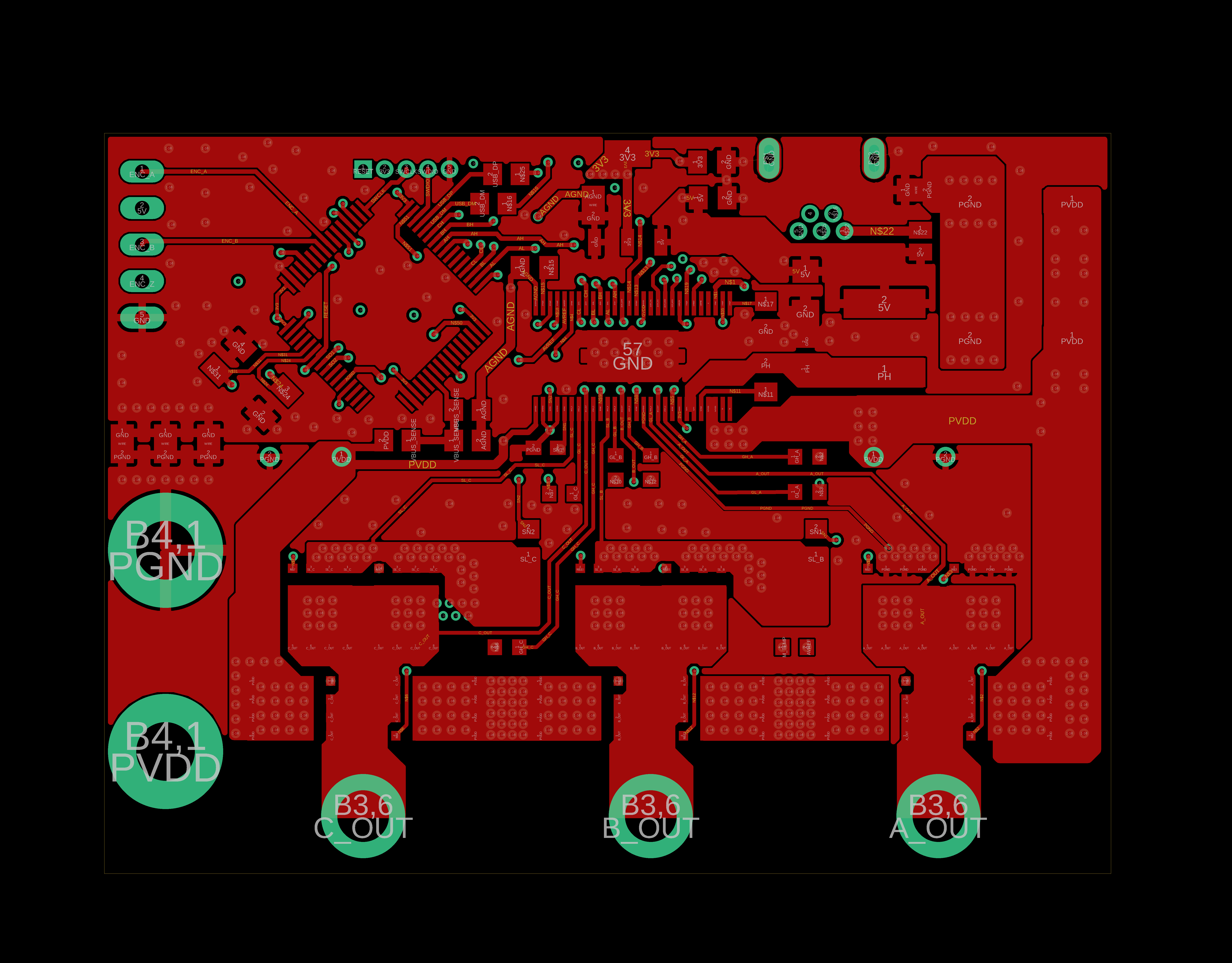
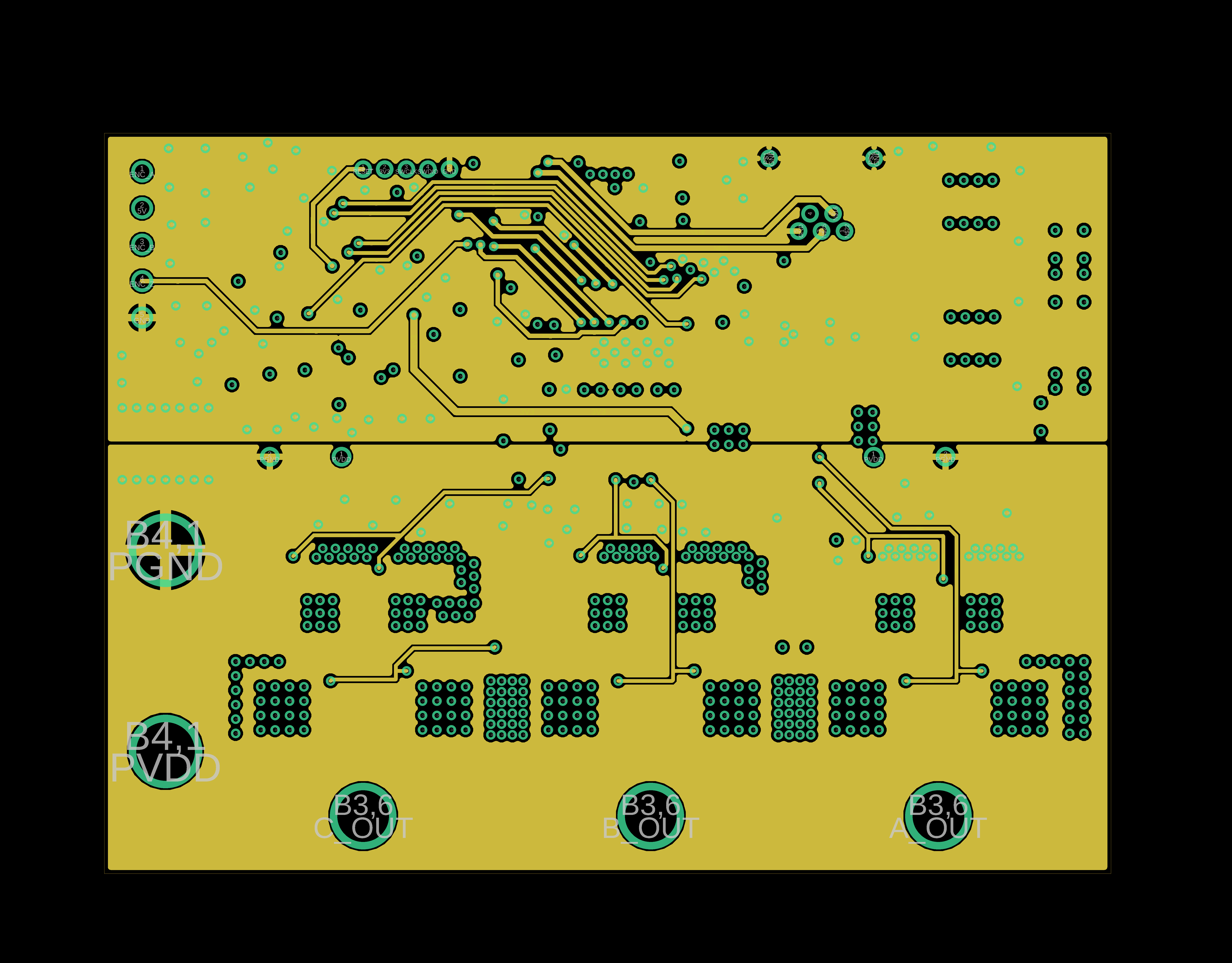
Layer 1 and 4 contain the high current traces, as well as the connections for most passive components, like those required for the DRV8301 and STM32.
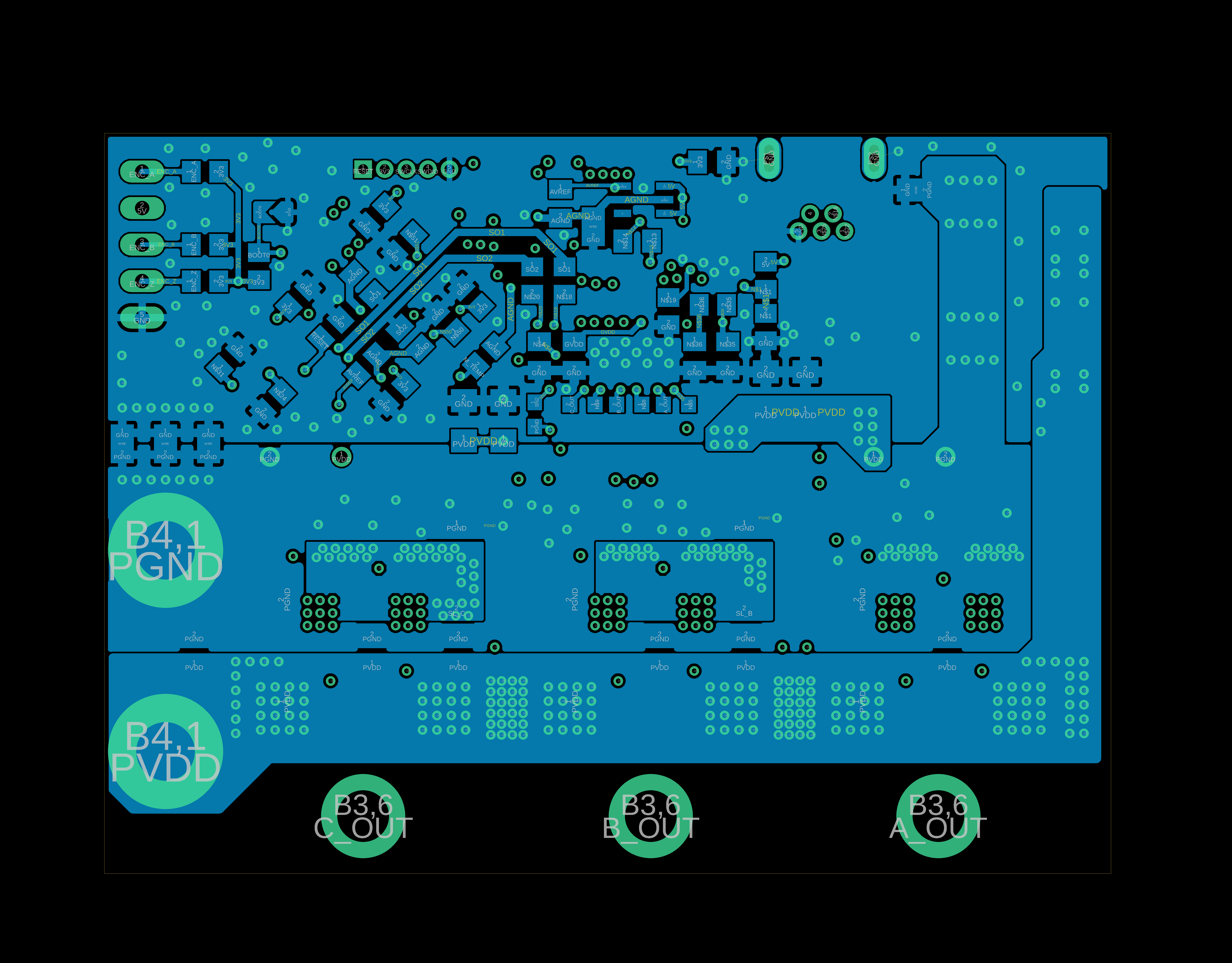
Layer 2 is where the majority of the switching signals are contained, including the SPI communication between the DRV8301 and STM32, USB data lines, and the STM32 gate control signals/DRV8301 gate outputs.
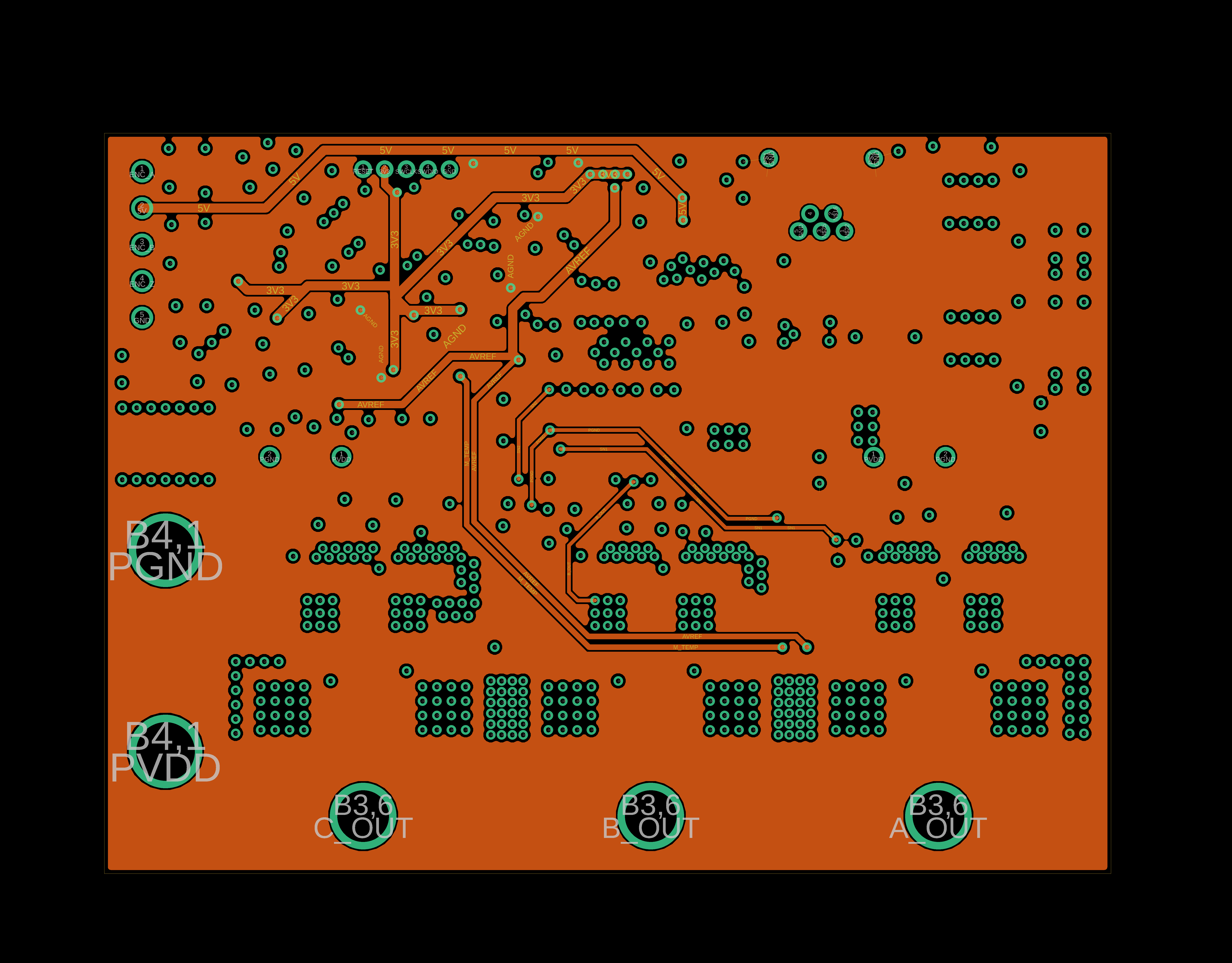
Layer 3 contains all the sensitive analog wires (current/temperature sense), as well as DC (5V, 3.3v analog VREF, and main 3.3v power) power distribution; the ground fill is the analog ground net, which is shorted to GND at the analog VREF regulator.
The files for this project can be found on my gitlab, currently it is a branch of the main BattleDriver project and can be found at: https://gitlab.elayne.me/eric/battle-driver/-/tree/BattleDriver+