The project was developed as a way to have small swappable motor drives that are capable of low to medium power systems. Ideally (with enough cooling) is capable of driving a robot in the weight range of 1 to 5lb. The board has support for dual axes to run two motors from a single Blade Drive.
The project is based on the open source ODrive project firmware (https://github.com/madcowswe/ODrive), with a custom implemention and communication scheme; in addition to several alterations to support the different hardware and status LEDs.
The hardware interfaces with the main system over an edge connector; including the power supply, motor phases, encoder, and communication/control signals.
The board is controlled by an STM32 which handles all of the motor control tasks, while handling SPI communication between itself and the main system.
The motor drivers are using a DRV8316 developed by Texas Instruments. It has integrated phase mosfets/current sense resistor, current sense amplifiers on each phase, and various controllable parameters influencing the switching behavior. The IC supports up to 8A and 35V, able to supply each motor with nearly 300W of continuous power (limited by cooling and a low kv motor to utilize the full 35V input range).
The board has a total of seven addressable status LEDs, one which is used to indicate board/system level status or errors. Three LEDs are used per axis to indicate the status or errors of the power stage, the motion controller, and the overall axis.
The board footprint is 30mm x 93mm; with all components populated the maximum depth of the board is 7.6mm. The edge connector that goes on the main system board has a depth of 9mm, meaning that the limiting factor for tiling multiple Blade Drives side by side is the edge connector depth (and routing of signals).
One use case is for a small CNC motion system (3D printer scale), you can have several Blade Drives side by side, with a relatively low space requirement. With the benefit of replaceable motor drivers that can just be swapped in or out whenever needed.
The design of the PCB focused heavily on best routing to avoid signal interference between the analog signals (such as the current sense amplifiers or temperature sensor) and the switching digital signals going to the DRV8316 devices. Traces were kept perpendicular when on top of each other across the copper layers. In addition, one of the four copper layers is a dedicated ground net with no traces braking it up. The ground plane was also separated into an analog and digital ground, where the two meet at one point on the dedicated ground layer.
All of these precautions should help to reduce noise in the current sense lines, helping to have a more accurate measurement of the per phase currents which improves control efficiency and potentially allows for faster switching speeds.
In addition to PCB design to improve phase current sense signal quality, each line has a dedicated RC filter to further reduce noise going into the STM32 ADC.
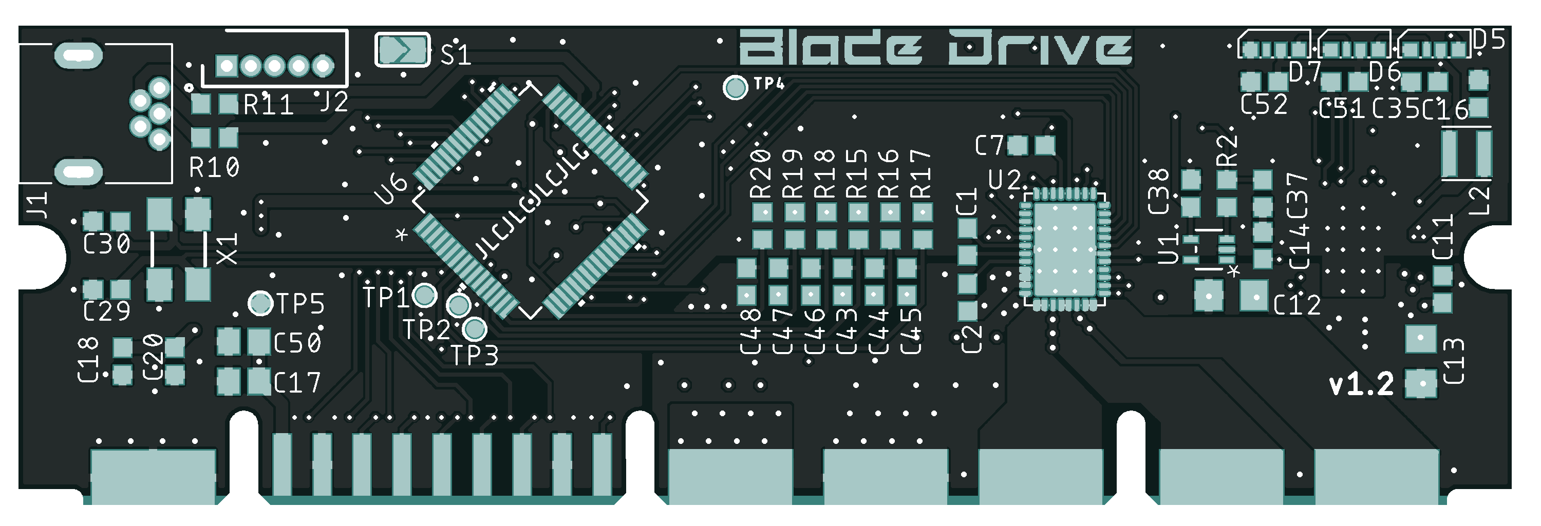
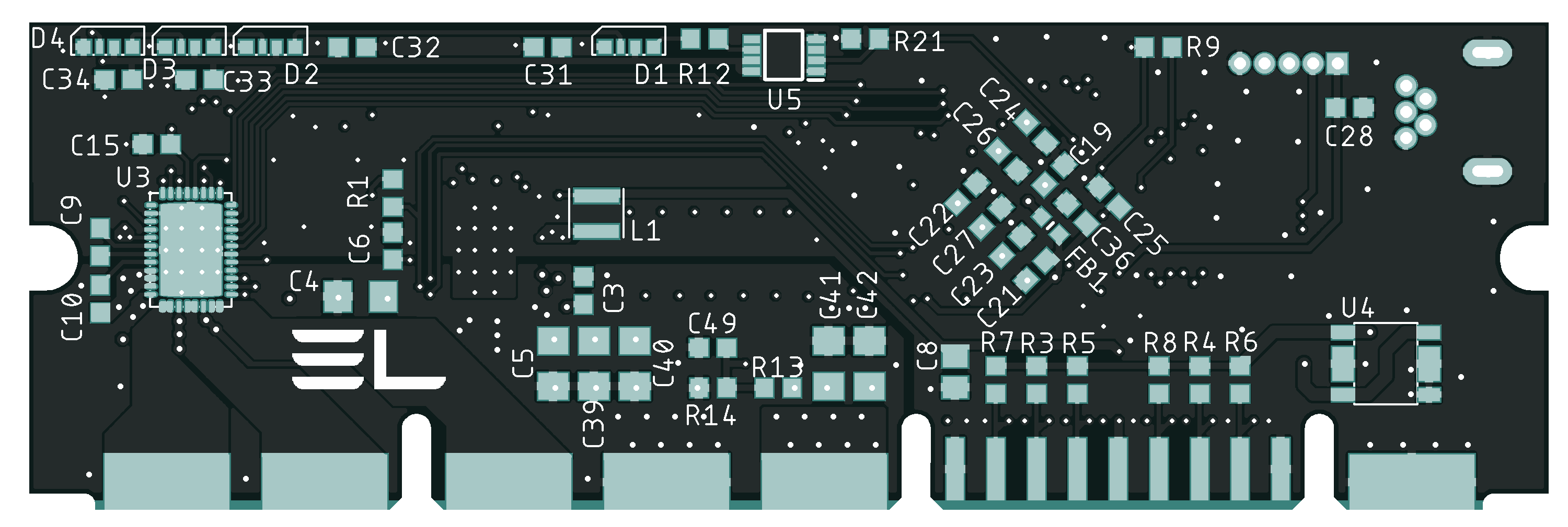
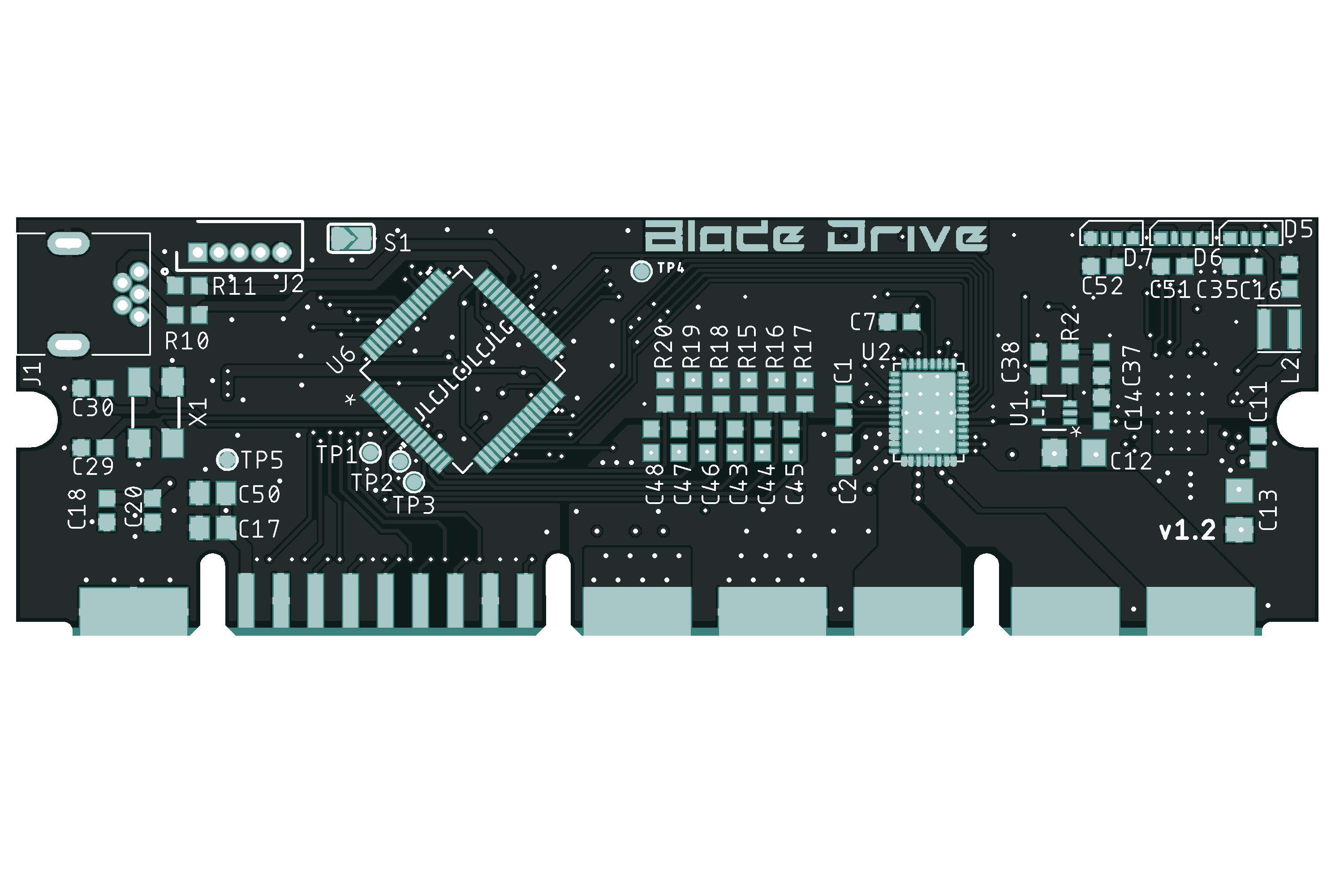
The board is shown below, note the actual board will have an ENIG surface finish and the exposed copper will be gold colored unlike in the preview: